
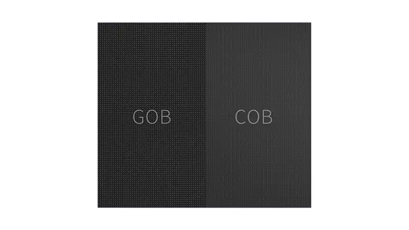
If you have ever tried to choose an LED video wall for a control room, a retail flagship, or a rental stage, you have probably run into two unfamiliar acronyms—COB and GOB. They sound similar, but they solve different problems and therefore fit different projects.
In this post, we’ll walk you through the COB LED display and GOB LED display, including how to choose the right one for your project and why it matters.
Table of Contents
1. Introduction
1.1 A 60-Second Primer on LED Displays
An LED display is a matrix of individual light-emitting diodes that are driven by driver ICs, controlled by a sender/receiver system, and mounted on a structural frame. By rapidly modulating the brightness of red, green, and blue dies, each pixel can produce the full color gamut. Over the last 15 years, LEDs have evolved from 20 mm through-hole lamps to 0.9mm SMD parts, and now to flip-chip microLED dies smaller than a grain of dust.
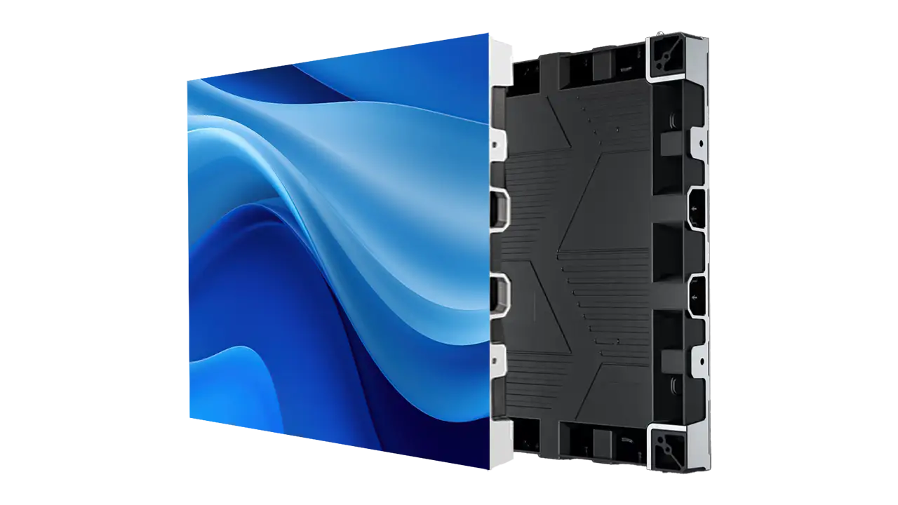
1.2 Why the Packaging Method Matters
The most visible part of an LED display is the front face, yet its reliability is determined by what happens behind and around each diode: heat extraction, mechanical protection, optical coupling, and electric interconnect. Packaging—the process that connects the bare chip to the PCB and shields it from the environment—dictates all of these factors.
Chip-on-Board (COB) and Glue-on-Board (GOB) are two competing packaging philosophies for small-pixel-pitch displays.
1.3 Purpose of This Post
- Demystify how COB and GOB are built.
- Compare them head-to-head on eight engineering metrics.
- List concrete advantages, disadvantages, and use cases.
- Offer a decision framework, FAQs, and reference links.
By the end, you should be able to specify the right technology for your next project—or at least challenge your supplier’s sales pitch with informed questions.
2. What Is a COB LED Display?
2.1 Definition
COB (Chip on Board) is a packaging technique in which bare LED dies are directly attached to a printed-circuit board, wire-bonded (or flip-chip soldered), and encapsulated in a uniform epoxy or silicone layer that becomes the visible surface. There are no discrete “lamp” packages; the PCB itself is the package.

For more information about flip chip COB LED screen, check this guide: Flip Chip COB LED Screen.
2.2 How COB Works—Step by Step
- Substrate Preparation
• FR-4, BT, or ceramic PCB with ENIG/OSP copper finish
• Thermal vias or metal-core inserts for heat spreading - Die Attachment
• Conductive epoxy or eutectic solder bonds the LED die to the copper pad.
• Automatic pick-and-place accuracy better than ±10 µm. - Wire Bonding / Flip-Chip Interconnect
• Traditional COB uses gold wire bonds; next-gen “IMD” uses direct flip-chip solder to eliminate wires and lower Z-height. - Underfill & Encapsulation
• A thin underfill secures the die; then a thicker optically clear epoxy floods the entire pixel matrix, filling micro-cavities and forming an unbroken lens. - Dicing into Modules
• The populated board is routed or laser-cut into panels such as 320 × 160 mm or 150 × 168.75 mm, or a big board 300 × 168.75 mm or 250 × 250mm.
2.3 Key Features
Generally, the COB LED screen has features as following:
• Seamless Surface – No solder mask openings or SMD leads; improves contrast.
• High Pixel Density – Pitches down to 0.4 mm today, roadmap below 0.2 mm.
• Efficient Heat Path – Die is less than 200 µm from copper; thermal resistance often < 5 K/W per pixel.
• Robustness – No individual lenses to crack and no pads to shear off; passes 5H pencil and 5 kg ball-drop tests.
• Optical Uniformity – Encapsulation acts as a shared diffuser, mitigating point-source glare and Moiré.
• Simplified BOM – Eliminates SMD carrier, reflow stencil, and paste.
• Maintenance Complexity – Requires micro-rework stations or full-module swap for dead pixels.
2.4 Pixel Pitch
The pixel pitch of a COB LED screen—defined as the center-to-center distance between adjacent LEDs—directly determines its achievable resolution and viewing distance. Smaller pitches like P0.78mm and P0.93mm pack more pixels per square meter, yielding ultra-fine detail suitable for close-up applications (e.g., broadcast walls and control rooms).
As you move to larger pitches such as P1.25 mm, P1.56 mm, and P1.875 mm, the pixel density decreases, which both lowers manufacturing costs and raises the optimal minimum viewing distance. Despite this, each pitch still delivers crisp imagery for medium-range installations like corporate lobbies or retail signage.
Below is a summary of common COB pixel pitches alongside their module and standard 600 × 337.5 mm panel resolutions (Here we use 300*168.75mm module as a reference):
| Pixel Pitch | Module Resolution (W × H) | Panel Resolution (W × H) |
| P0.78125 mm | 384 × 216 | 768 × 432 |
| P0.9375 mm | 320 × 180 | 640 × 360 |
| P1.25 mm | 240 × 135 | 480 × 270 |
| P1.5625 mm | 192 × 108 | 384 × 216 |
| P1.875 mm | 160 × 90 | 320 × 180 |
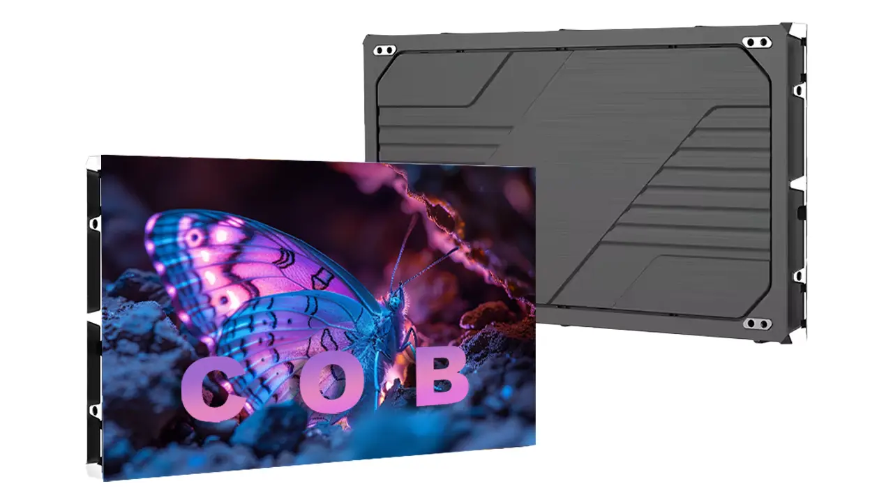
3. What Is a GOB LED Display?
3.1 Definition
GOB (Glue on Board) is a protective overlay process applied to conventional SMD modules. After the SMD LED packages are reflow-soldered, a transparent, UV-curable resin is dispensed across the entire face, filling the gaps between LEDs and forming a durable “gasket.”

3.2 How GOB Works—Step by Step
- Standard SMD Assembly
• Uses the same pick-and-place, reflow, and AOI process as any indoor LED panel. - Plasma Cleaning
• Removes flux residues that would compromise adhesion. - Resin Dispensing / Vacuum Filling
• A two-part silicone or modified epoxy is metered onto the module; vacuum draws resin underneath the package flanges. - Curing
• UV or thermal bake polymerizes the resin into a tough elastomer 0.2 – 0.5 mm thick. - Surface Finishing
• Optional matte texturing reduces reflections; laser cutting exposes test pads.
3.3 Key Features
• Eight-Way Protection – Water, dust, mechanical impact, ESD, salt-spray, blue-light filtering, oxidation, vibration.
• Cost-Effective Upgrade – Adds ± 8 % cost to existing SMD line, versus 20 – 30 % cap-ex for COB flip-chip equipment.
• Field Serviceability – Dead LEDs can still be hot-tweezed once resin is locally heated.
• Optical Smoothness – Point-to-surface conversion improves contrast and eliminates lensing artifacts.
• Pixel Pitch Floor – Limited by SMD leadframe geometry; practical minimum ≈ 0.9 mm today. It supports most indoor LED modules such as P2, P2.5, P2.604, P1.976, P1.95, P3.91, P3, P4, P5, P3.075, P1.538, P1.86
4. COB vs GOB: Head-to-Head Comparison

Here’s a concise yet comprehensive comparison of COB and GOB LED displays, structured for clarity and technical accuracy:
| Metric | COB | GOB | Comment |
|---|---|---|---|
| Brightness | 800 – 1 600 nits indoor; 3 000 + outdoor (with common-cathode) | 600 – 1 400 nits indoor | Resin absorbs ~3–5 % light. |
| Contrast Ratio | 10000 : 1 (with matte black epoxy) | 8000 : 1 or 10000:1 | Both higher than bare SMD (~5 000 : 1). |
| Durability | IK06/07; survives finger nails, carts, and light hammer | IK07/08; resin acts as shield | GOB slightly better against point impact. |
| Waterproof / Dustproof | IP54 front (encapsulant), IP65 rear possible | IP65 front; front can be hosed | GOB wins for outdoor. |
| Visual Performance | Pixel pitch as low as 0.4 mm; no Moiré under camera | Pitch ≥ 0.9 mm; mild lensing | For broadcast, COB dominates. |
| Maintenance | Whole-module swap or micro-rework | Single LED hot-swap possible | Service cost lower on GOB. |
| Cost | $1400/m² @ P1.25; up-charges for < 0.9 mm | $1000/m² @ P1.5 | < P1.0 only available in COB today. |
| Lifespan | > 100000 h L50 under 25 °C | 80000–100000 h L50 | Resin yellowing after 7–10 yrs may reduce blue output. |
5. Advantages and Disadvantages
After we have learned the basic concept of COB LED display and GOB LED display, let’s move ahead to the pros and cons.
5.1 COB Advantages
- Ultra-fine pixel pitch down to micro-LED territory.
- Superior heat dissipation, enabling higher maximum brightness without derating.
- Flat, lens-free surface eliminates Moiré and reduces specular glare.
- Excellent mechanical stability for touch-interactive or rental floors.
- Simplified supply chain (no SMD carrier, no reflow oven).
5.2 COB Disadvantages
- Expensive capital equipment (flip-chip bonders, plasma cleaners, total AOI).
- Pixel-level repair is difficult; full-module replacement increases spares inventory.
- Still maturing—industry lacks uniform reliability standards for encapsulant aging.
- Limited third-party vendors; risk of vendor lock-in.
- The price is very expensive
For more information about the COB LED Screen price, check this.
5.3 GOB Advantages
- Drastically higher IP rating than naked SMD without redesigning the electronics.
- Maintains conventional SMT workflow; easy to adopt for existing factories.
- Field-repairable with hot tweezers and fresh resin.
- Better impact resistance than SMD and almost as good as COB.
- Price premium is small at pixel pitches > 1 mm.
5.4 COB Disadvantages
- Pixel pitch cannot realistically drop below 0.9 mm.
- Resin introduces a slight optical loss and potential yellow shift over a decade.
- Added thermal resistance requires conservative current driving.
- Improper curing can cause stress cracks or delamination.
5. Which Should You Choose?
After understanding the strengths and weaknesses of COB and GOB LED displays, here is the question: which should I choose when building a LED video wall?
The best choice depends on your specific needs and viewing conditions. Here’s a quick guide:
1. Prioritize COB If You Need:
- Ultra-Fine Pixel Pitch (< 0.9 mm) for close-up viewing (e.g., control rooms, broadcast studios).
- Superior Heat Dissipation for high-brightness applications (3,000+ nits).
- Seamless, Glare-Free Display (ideal for camera-facing environments).
- Long-Term Reliability with minimal maintenance (though repairs are harder).
2. Opt for GOB If You Need:
- Durability in Harsh Conditions (waterproof, dustproof, impact-resistant for outdoor/rental use).
- Easier & Cheaper Repairs (individual LED replacement possible).
- Cost-Effective Solution for pitches ≥ 1.0 mm (e.g., corporate lobbies, digital signage).
- Wider Viewing Angles (near 180° with resin diffusion).
3. Key Considerations:
- Viewing Distance:
- < 2m? COB (P0.9–P1.2) for sharpness.
- > 3m? GOB (P1.5+) saves costs without sacrificing clarity.
- Environment:
- Humid/dusty? GOB’s IP65 rating wins.
- Touch-interactive? COB’s rugged surface is safer.
- Budget:
- COB = premium pricing for cutting-edge tech.
- GOB = affordable protection for SMD-based displays.
Final Advice: Match the technology to your use case, budget, and environment. For mission-critical, high-resolution needs, COB is unmatched. For tough, service-friendly displays, GOB delivers.
- Choose COB for ultimate resolution, high brightness, and premium installations where upfront cost is less important than image fidelity.
- Choose GOB when you want SMD economics plus a protective “windshield” for rough handling or damp environments.
6. Conclusion
COB and GOB both represent evolutionary steps beyond bare SMD, but they originate from different engineering goals—COB pursues ultra-fine pitch and thermal efficiency, whereas GOB pursues ruggedization and environmental sealing.
Understanding their construction clarifies why COB dominates sub-millimeter, camera-facing applications, while GOB thrives in rental and outdoor scenarios. Match their strengths to your project’s pixel pitch, durability needs, service model, and budget, and you will seldom choose wrong.
In this post, we have explored everything you need to know about COB LED and GOB LED screens, from concepts to the differences. If you still don’t know which to choose, you can contact us at any time, and we will offer the best solution to help you choose.
7. Frequently Asked Questions
Is COB the same as microLED?
No. MicroLED refers to die size (< 50 µm) and self-emissive architecture, whereas COB refers to how any size die—micro or conventional—is mounted on the board.
Can a GOB panel be converted to COB later?
Practically no. GOB starts with packaged LEDs; COB uses bare dies. Converting would require scrapping the module.
Why are COB repairs hard?
Bare dies are tiny (50–100 µm). Replacing one requires a micro-bonder, microscope, and low-void encapsulation. Most owners stock spare modules instead。
Which has lower power consumption?
Electrical efficiency is mostly a function of LED epi and driver IC. COB can run cooler at the same brightness, allowing you to dim slightly and save 5–10 % energy.


